Root Interface Condition Analysis
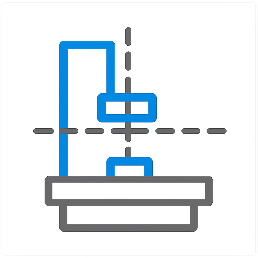
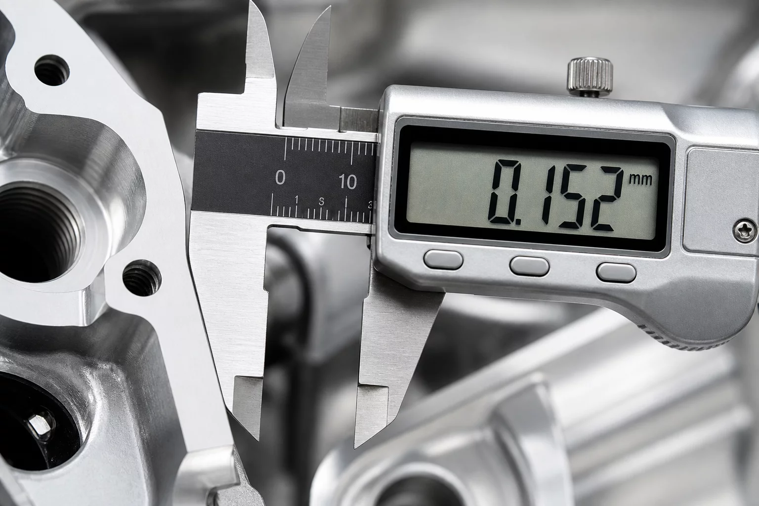
In precision mechanical design, confusing nominal clearance with manufacturing tolerance stack-up is among the most frequent culprits behind physical assembly interference. Clearance represents the intended geometric offset deliberately modeled between adjacent mating surfaces to enable relative movement, structural insertion, or fluid flow. Conversely, tolerance defines the permissible dimensional deviation from nominal geometry created by fabrication methods such as CNC milling, casting, or 3D printing. When CAD engineers assume manufactured components will exist at perfect nominal values, the accumulated variation across multiple mating features inevitably leads to tight binding or unwanted mechanical play.
A designed 0.25 mm clearance gap between locating pin shoulders and surrounding housing flanges ensures smooth sliding insertion during single-operator manual assembly.
Cumulative upper-bound fabrication tolerances (+0.15 mm pin diameter, -0.12 mm pocket depth) fully eliminate clearance, generating severe binding during joint engagement.
Dimensional & Tolerance Interplay
Resolving tolerance stack-up conflicts requires rigorous analysis of worst-case boundary conditions alongside geometric dimensioning and tolerancing (GD&T) principles. When clearance holes for fasteners are mistakenly used for precision location instead of dedicated dowel pins, lateral positioning wanders significantly. By decoupling primary datum locating features from threaded clamping interfaces, designers allow generous fastener clearance while preserving the exacting sub-millimeter positional repeatability demanded by functional mechanisms.